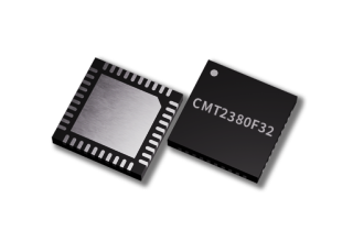
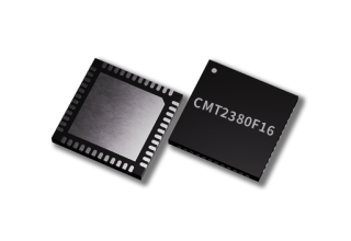
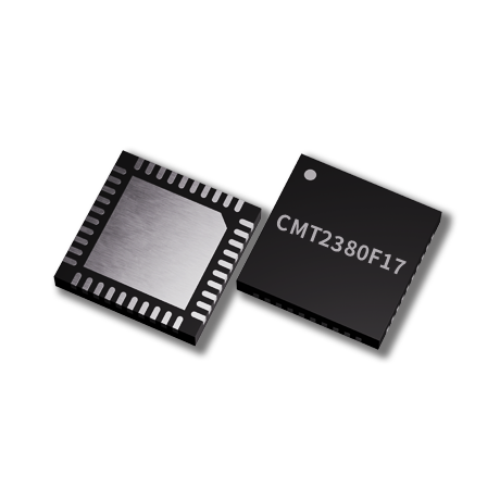
Ultra Low Power Sub-1GHz Wireless MCU
Description
Employed an 8-bit CPU core and an ultra-low power RF transceiver, the CMT2380F17 is a (G)FSK, (G)MSK, and OOK wireless MCU with high performance and ultra-low power applying to 127 to 1020 MHz band wireless applications. Operating with 1.8 to 3.6 V supply voltage, the CMT2380F17 consumes only 72 mA transmission current and 8.5 mA (exclusive of MCU consuming) receiving current while delivering up to 20 dBm power and reaching -121 dBm sensitivity.
The device employs a wide range of peripherals like support of standard UART, I2C and SPI interfaces, up to 25 general-purpose I/Os, support of internal high-speed, low-speed, low-power RC oscillators and 32.768 kHz external crystal oscillators, flexible data handling and packet handler, up to 64-byte Tx/Rx FIFO, feature-enriched RF GPIO, multiple low-power modes and fast-start mechanisms, high-precision RSSI, manual fast frequency hopping, multi-channel input 12-bit high-speed ADC, etc. Leading the industry in the aspect of the smallest package size, the CMT2380F17 is ideal for IoT applications with critical requests in size constraints and power-efficiency.
MCU Features
1-T 80C51 CPU platform
16kB program area Flash with password access protects. Default space configuration:
- AP program space (13.5 kB, 0000h ~ 35FFh)
- IAP data space (1.0 kB, 3600h ~ 39FFh)
- ISP boot code space (1.5 kB, 3A00h ~ 3FFFh)
1 kB data memory
- 256-byte high-speed buffer
- 768-byte of extended RAM (XRAM)
- Extended RAM (XRAM) supporting page access
On-chip debug interface (OCD)
Multiple power control modes: power-down mode, idle mode, slow-frequency mode, sub-frequency mode, RTC mode, watch mode, and monitor mode
- All interrupts supporting to wake up the CPU from IDLE mode
- 10 interrupt sources supporting to wake up the CPU in power-down mode
- Slow-frequency mode and sub-frequency mode supporting low-speed MCU operation
- RTC mode supporting real-time clock (RTC) to wake up the CPU in power-down mode
- Watch mode supporting watchdog (WDT) to wake up the CPU in power-down mode
- Monitor mode supporting BOD1 to wake up the CPU in power-down mode
Operating frequency range: up to 25 MHz
- External crystal oscillator mode, 0–12 MHz at 2.0–3.6 V and 0–25 MHz at 2.4–3.6 V
- CPU operating frequency can reach 12 MHz at 1.8-3.6 V and 25 MHz at 2.2-3.6 V
- When on-chip clock frequency multiplier (CKM) is at 2.7–3.6 V, the CPU operating frequency
can reach 36 MHz.
Double data pointer
Interrupt control
- 16 interrupt sources, 4 priority levels
- 3 external interrupts nINT0/1/2, with filtering
- All external interrupts supporting high/low or rising/falling edge triggering
8-channel 12-bit single-ended ADC with a sampling rate greater than 500 ksps
1 master/slave SPI serial interface, the rate reaching 12 MHz
2 master/slave two-wire serial interfaces: TWI0/I2C0 and STWI (SI2C)
1-channel DMA engine
- P2P, M2P, P2M
- Memory target: XRAM
- Peripheral targets: UART0, UART1, SPI, TWI0/I2C0, ADC12 and CRC16
- Timer 5 and Timer 6 are applied by DMA; they are independent timers when DMA is not
enabled.
Totally 9/11 timers/counters on-chip
- RTC timer and WDT timer
- Timer 0, 1, 2, 3
- PCA0, programmable counter array 0
- S0BRG and S1BRG
- When timer 2/3 is used in separated mode, there are a total of 11 timers
8 keyboard interrupts
1 enhanced UART0 and 1 normal UART1
RF Features
Operating frequency: 127-1020 MHz
Modulation and demodulation methods: (G)FSK, (G)MSK, OOK
Data rate: 0.5-300 kbps
Sensitivity: -121 dBm @ 434 MHz, FSK
Receive current: 8.5 mA @ 434 MHz, FSK
Transmitting current: 72 mA @ 20 dBm, 434 MHz
Configurable FIFO up to 64-Byte
System Features
Operating voltage: 1.8 – 3.6 V
Operating temperature: -40 – 85 ℃
QFN40 5x5 packaging
Application
Automatic meter reading
Home security and building automation
Wireless sensor networks and industrial monitoring
ISM band data communication